把512 GiB闪存搬到xPU旁边,HBF能打破推理内存墙?
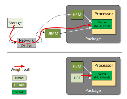
TL;DR - SK hynix and SanDisk published the OCP "High Bandwidth Flash (HBF) High-Level Base Die Specification v0.7.0", defining a non-coherent, memory-centric NAND device co-packaged next to GPUs/TPUs to add TB-scale capacity between HBM and SSD. It matters because inference is increasingly capacity-bound (weights, KV cache, MoE, multi-model), not just bandwidth-bound.
- Architecture: Base Die + stacked NAND core dies + TSVs; host connects over UCIe 3.0 with AXI as the transaction protocol. The Base Die handles NAND commands, ECC, scheduling, error reporting and TSV redundancy — it is not a passive interposer.
- Performance: reference config is 16 NAND dies, 16 banks/channel, 4 KiB pages, 512 GiB total; up to 16 independent host channels, 64-bit each at up to 32 GT/s per lane, yielding a spec target of ~3 TB/s. That figure is aggregate parallelism at max configuration, not measured silicon.
- Workloads extend beyond static weights to KV cache, MoE, multimodal and agentic serving; multi-model layouts can either interleave across all channels (max bandwidth) or dedicate channel groups (isolation).
- Key tradeoff: NAND constraints remain — 4 KiB-aligned sequential writes within a block, erase-before-rewrite, endurance limits. Channels have separate address spaces and HBF must be managed separately from HBM, so the host software owns global-to-channel mapping, weight/KV-cache partitioning, and part of wear leveling.