都叫3D芯片,为什么是三门不同的生意?
Ranking
No observed public metrics; popularity remains neutral/archived.
Merged summary
TL;DR - A Chinese tech-media analysis of the current "3D stacking" AI-chip investment wave, arguing that the shared label actually covers three distinct businesses with different markets, engineering hurdles, and validation criteria. It matters because agentic/long-context inference is shifting the chip bottleneck from peak FLOPS to memory capacity, bandwidth, and data movement.
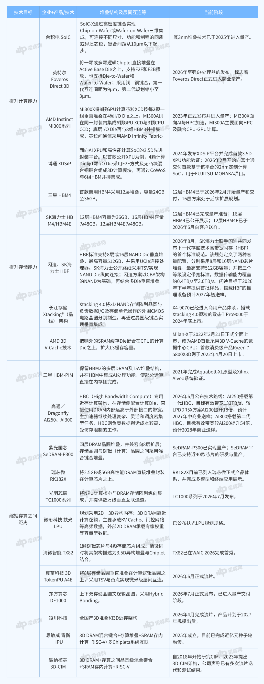
- Three distinct 3D routes are conflated: (1) logic-chiplet recombination (TSMC SoIC, Intel Foveros, AMD MI300) to sustain scaling as advanced nodes get costly; (2) memory-side expansion (HBM, HBF, 3D V-Cache) targeting bandwidth, capacity, and cache hierarchy; (3) vertical logic-DRAM integration or compute-in-memory (Ziguang Guoxin, Rockchip, Samsung HBM-PIM, plus startups) that changes where compute sits.
- Agent workloads lengthen inference into sustained multi-call tasks; the decode phase repeatedly reads weights and KV cache, so compute and bandwidth demands diverge and general-purpose GPUs stop being cost-optimal for that stage.
- Chinese startups favor logic-memory vertical integration because 3D memory competition requires DRAM/NAND wafer fabs (Samsung, SK Hynix, Micron, CXMT, YMTC) and chiplet routes need mature die-to-die and software ecosystems; they stack at ~7nm rather than 3/2nm, using architecture to offset process gaps.
- Cited practical limits: heterogeneous compute+memory stacks face uneven stress, warpage, thermal and yield issues, making roughly 4-6 layers realistic today; success requires proving decode (ideally attention operators) on real silicon with high TPS, plus a full software stack (ISA, compiler, runtime, operator libraries) — several firms are pre-tape-out yet already valued in the tens of billions of RMB.
Sources (1)
都叫3D芯片,为什么是三门不同的生意?
TL;DR - A Chinese tech-media analysis of the current "3D stacking" AI-chip investment wave, arguing that the shared label actually covers three distinct businesses with different markets, engineering hurdles, and validation criteria. It matters because agentic/long-context inference is shifting the chip bottleneck from peak FLOPS to memory capacity, bandwidth, and data movement.
- Three distinct 3D routes are conflated: (1) logic-chiplet recombination (TSMC SoIC, Intel Foveros, AMD MI300) to sustain scaling as advanced nodes get costly; (2) memory-side expansion (HBM, HBF, 3D V-Cache) targeting bandwidth, capacity, and cache hierarchy; (3) vertical logic-DRAM integration or compute-in-memory (Ziguang Guoxin, Rockchip, Samsung HBM-PIM, plus startups) that changes where compute sits.
- Agent workloads lengthen inference into sustained multi-call tasks; the decode phase repeatedly reads weights and KV cache, so compute and bandwidth demands diverge and general-purpose GPUs stop being cost-optimal for that stage.
- Chinese startups favor logic-memory vertical integration because 3D memory competition requires DRAM/NAND wafer fabs (Samsung, SK Hynix, Micron, CXMT, YMTC) and chiplet routes need mature die-to-die and software ecosystems; they stack at ~7nm rather than 3/2nm, using architecture to offset process gaps.
- Cited practical limits: heterogeneous compute+memory stacks face uneven stress, warpage, thermal and yield issues, making roughly 4-6 layers realistic today; success requires proving decode (ideally attention operators) on real silicon with high TPS, plus a full software stack (ISA, compiler, runtime, operator libraries) — several firms are pre-tape-out yet already valued in the tens of billions of RMB.